Discussion
Loading...

Post

Log in
  • About
  • Code of conduct
  • Privacy
  • Users
  • Instances
  • About Bonfire
DJ🌞:donor:
DJ🌞:donor:
@infosecdj@infosec.exchange  ·  activity timestamp 2 days ago

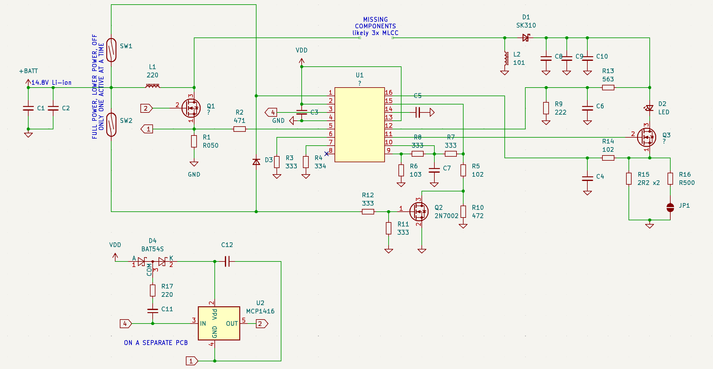
Hey #electronics folks. Here's my situation. I got a wintertime project this week, and it's a busted diving light. Its driver PCB self-immolated inside the light's head. Here is what I managed to reconstruct; the manufacturer was an ass enough to remove markings from active components. In that regard, I got a couple questions which I can't figure out myself.

1. I get there is no figuring p/n for FETs, but maybe anyone has an idea what the controller chip might be?
2. Any idea on why D4/R17/C11 were included?
3. How should I go around finding a replacement for those FETs?

Any help will be appreciated!

Reconstructed schematics; no big point in trying to describe it.
  • Copy link
  • Flag this post
  • Block
Joel Michael
Joel Michael
@jpm@aus.social replied  ·  activity timestamp 2 days ago

@infosecdj #2 looks like it’s forming a R-C delay circuit, without connecting the GPIO directly to VCC. My guess is the “low power” mode is PWM, which also explains the MOSFET gate driver.

#3 for first step you need to find N-channel MOSFETs with the correct footprint and pin order. The high-power-mode MOSFET will need careful consideration with its safe operating area at DC, keeping the V and I inside the SOA curve, the low-power-mode may need more consideration around the t(rise) and t(fall) parameters depending on the pulse width of the PWM signal because the SOA is larger at lower duty cycles than DC

  • Copy link
  • Flag this comment
  • Block
DJ🌞:donor:
DJ🌞:donor:
@infosecdj@infosec.exchange replied  ·  activity timestamp 2 days ago

@jpm The low power mode, as I understand it, just engages SW2, which turns Q2 on, which shunts R10, in turn likely changing voltage/current setting for the driver. PWM is done via Q3 already, Q1+L1+L2+D1+blown MLCCs form a SEPIC converter. That much is known.

(I still don't understand why PWM is done on a non-inductive load to control current... but it seems a lot of people believe this is the way)

  • Copy link
  • Flag this comment
  • Block
ozeng
ozeng
@ozeng@aus.social replied  ·  activity timestamp 2 days ago

@jpm @infosecdj #2 is classic snubber topology, usually it’s for EMI filtering. If they’d just wanted to slow the mosfet the usual way is a single gate resistor to work against the fet’s built-in gate capacitance. No idea by the diodes, maybe trying to constrain the pixies from propagating elsewhere but looks a bit unusual. They’re either a much better engineer than me or a much worse engineer than me but I have no idea which one is true.

  • Copy link
  • Flag this comment
  • Block

bonfire.cafe

A space for Bonfire maintainers and contributors to communicate

bonfire.cafe: About · Code of conduct · Privacy · Users · Instances
Bonfire social · 1.0.1-alpha.40 no JS en
Automatic federation enabled
Log in
  • Explore
  • About
  • Members
  • Code of Conduct