

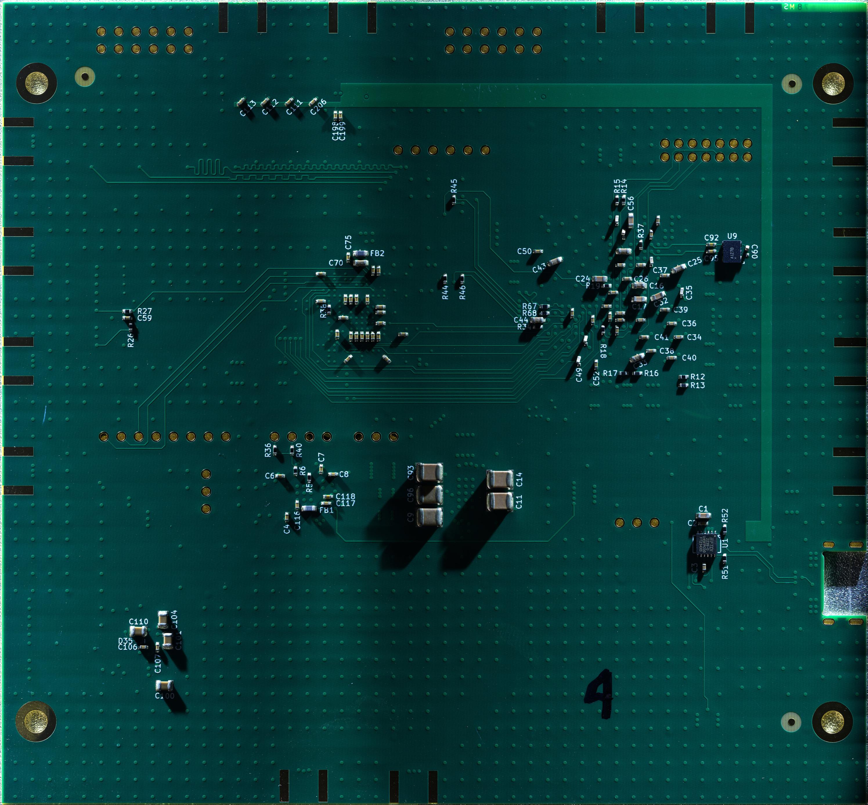
I'll post representative images of some defects later on, but from a first pass looking at the full res photos, I see 5 defects, mostly clustered in the northeast.
There's a higher than normal rate of defects since this board wasn't done in my home oven using my own highly tuned process, but at the local catgirl polycule's shop since I was using their PnP (which I own a 20% stake in).
Something about the process seems off and I want to understand what, since this is a line I expect to be using a lot more and I want to fix any process issues to improve yields on the next batch. So rather than just fixing issues I'm trying to get photos and data of all of them.
* C58 tombstoned, north side making contact
* C90 tombstoned, north side making contact
* C51 tombstoned, north side making contact
* C3 tombstoned, north side making contact
* R13 slightly misaligned, east side a bit displaced south of nominal but probably still OKish
R68 also has a bit of solder paste debris on the top but I'm ignoring that because it was a hand placed part that I remember messing up.
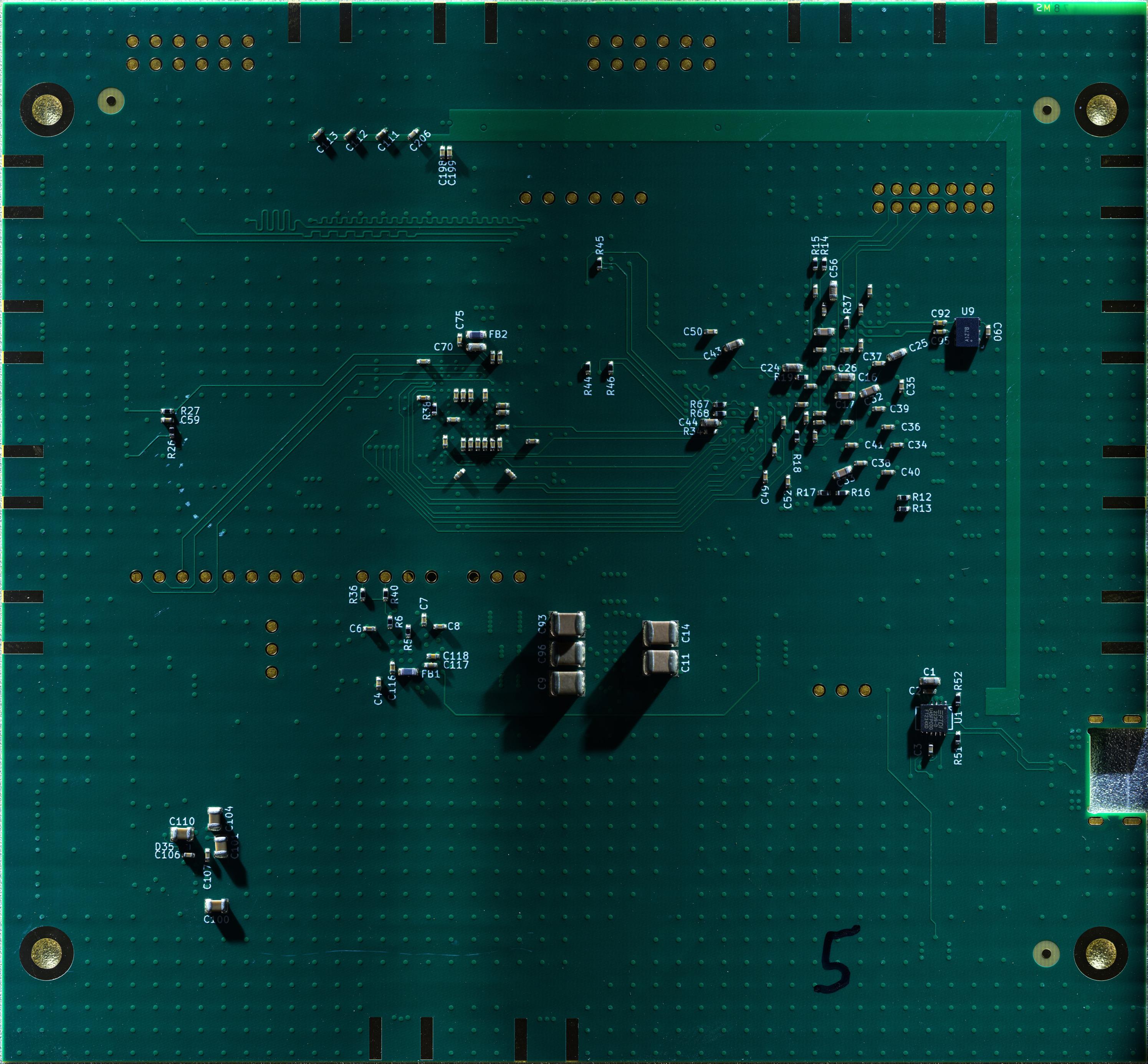

Board number 3 has five defects:
* C3, C55, C90 tombstoned, north side making contact
* Mid-chip solder ball on C2, R13