

Okay FINE I’ll increase the schematic drawing borders to A2 size
0 Boosts
0 Likes
@ozeng that’s the nice* thing about modern EDA tools, you aren’t constrained by the size of a single piece of paper. Yeah you might start on a single sheet, but then bits get added and splatted down everywhere before being cleaned up later

@jpm we are spoiled for tools these days, it’s amazing.
I unfortunately deal with circuits drawn by someone who had the tools but didn’t know how to use them effectively. Off-page connectors don’t exist, missing connections on the schematic, etc. The schematic and PCB were done separately without parity checking. Had to drill out and bodge-wire a signal trace that was connected to ground (it’s in the layout, it was an accident in design).
I’m sure my CAD work is reproachable too but.. there are levels man 😅


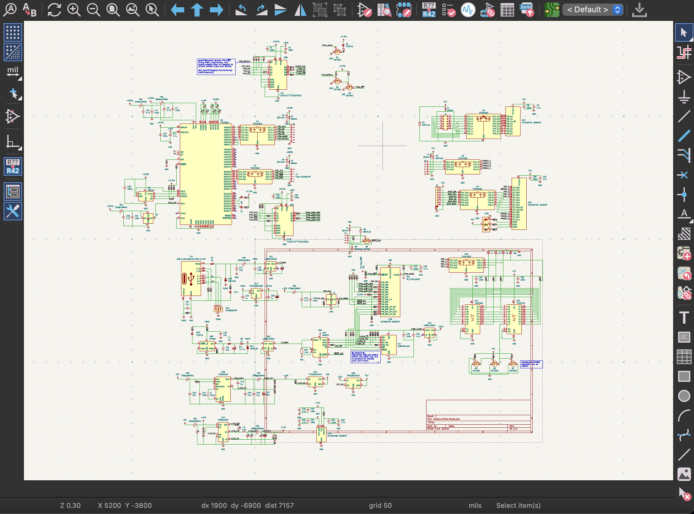

@jpm maybe I should split this over multiple pa… fuck it, too hard. A2 it is!