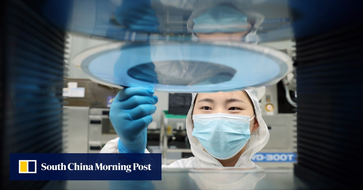

A Chinese research team has achieved a potential breakthrough in chipmaking, developing a method that reduces lithography defects by up to 99%.
Using cryo-electron tomography, they pinpointed the sources of manufacturing flaws. The solution is compatible with existing production lines for 12-inch wafers, promising significant cost savings for the global semiconductor industry.